◎
Multiple Disciplines
PCB, package, mechanical, thermal, SI, PI, and more.



Integration & Systems Authority
SAS Advanced Technologies delivers expert high speed PCB and IC substrate design, SI and PI simulation, 112G PAM4 engineering, and production-driven execution from concept through manufacturing
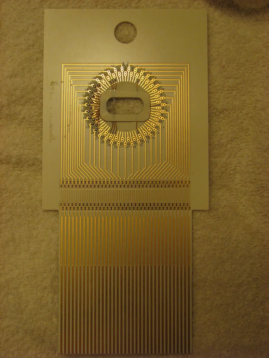

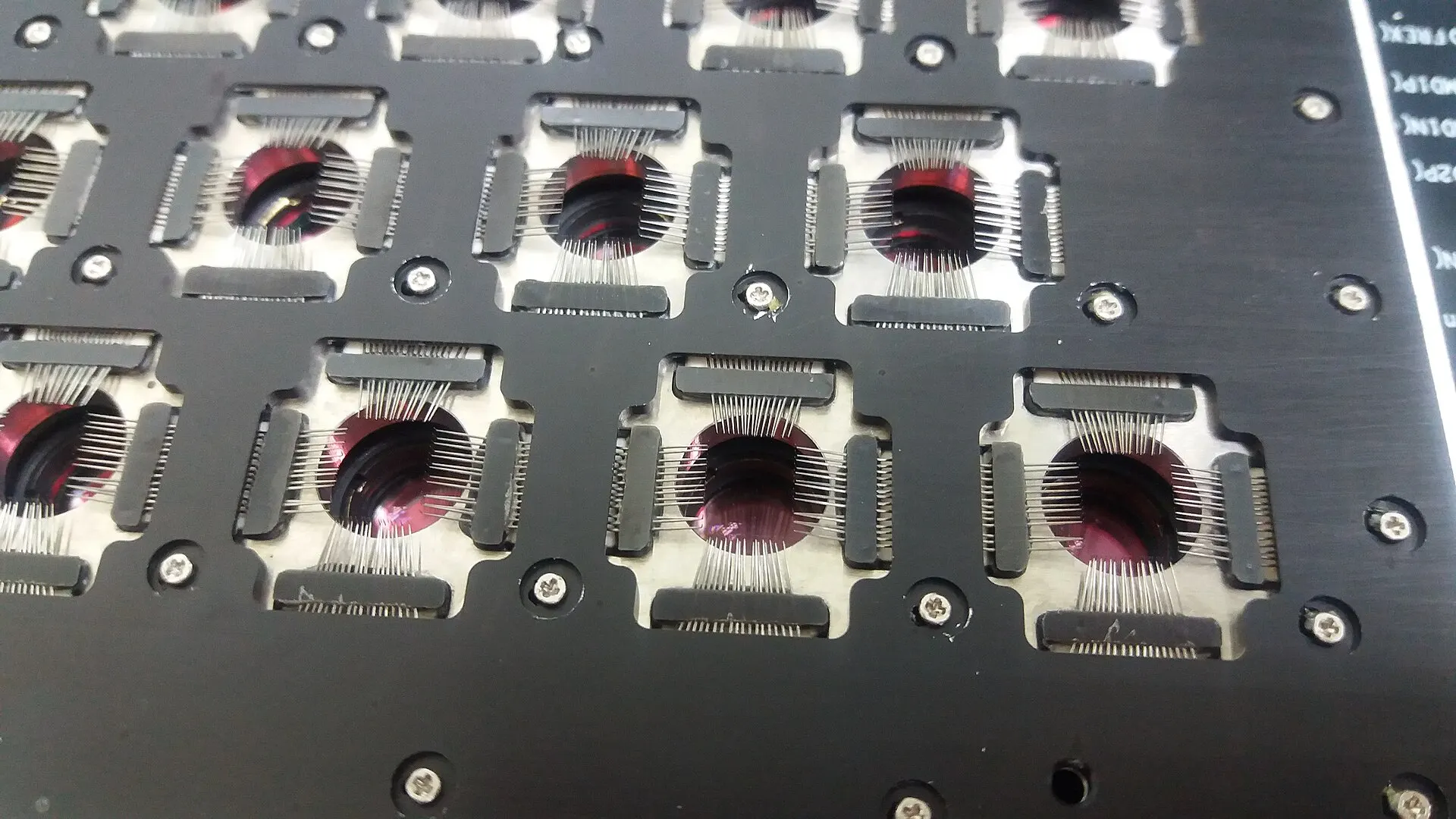
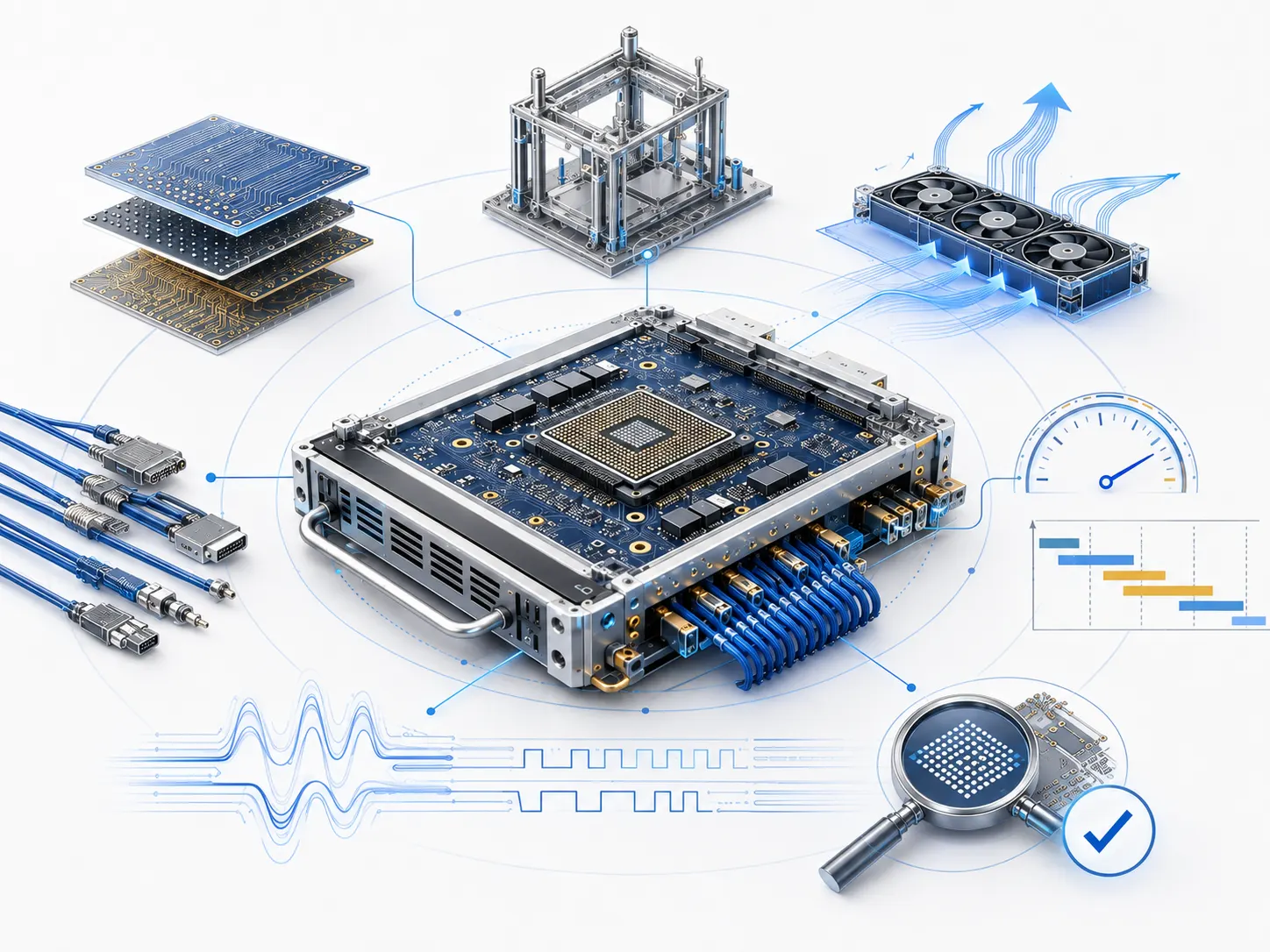
The Challenge
Advanced test hardware involves multiple engineering disciplines, manufacturers, interfaces, and technical dependencies. When these activities are managed separately, projects become slower, less predictable, and harder to control.
PCB, package, mechanical, thermal, SI, PI, and more.
Electrical, mechanical, firmware, and system-level interfaces.
Programs demand speed, accuracy, and predictability.
Quality and reliability directly affect your product.
SAS provides one coordinated engineering and delivery process.
Why SAS
We own the program from requirements to delivery.
Design decisions reflect manufacturing and production constraints.
Specialized international partners combined with direct local support.
Experience across compute, networking, automotive, sensing and advanced systems.
Engineering Domains
SAS delivers deep engineering capabilities across the full hardware lifecycle, from design and simulation through manufacturing and production execution.
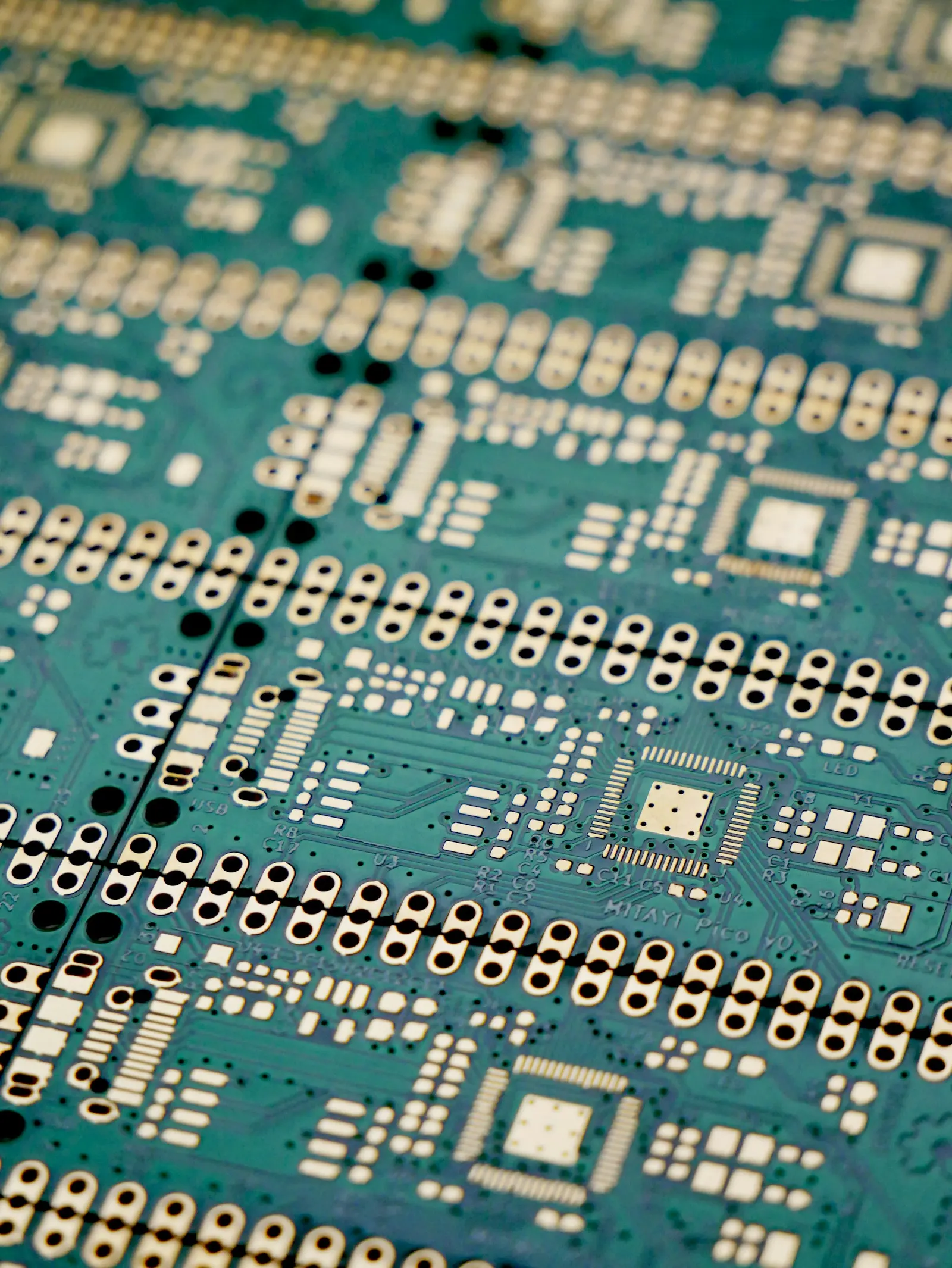
Constraint-driven multilayer PCB engineering for high speed compute, RF, mixed-signal, and advanced semiconductor platforms.
Explore domain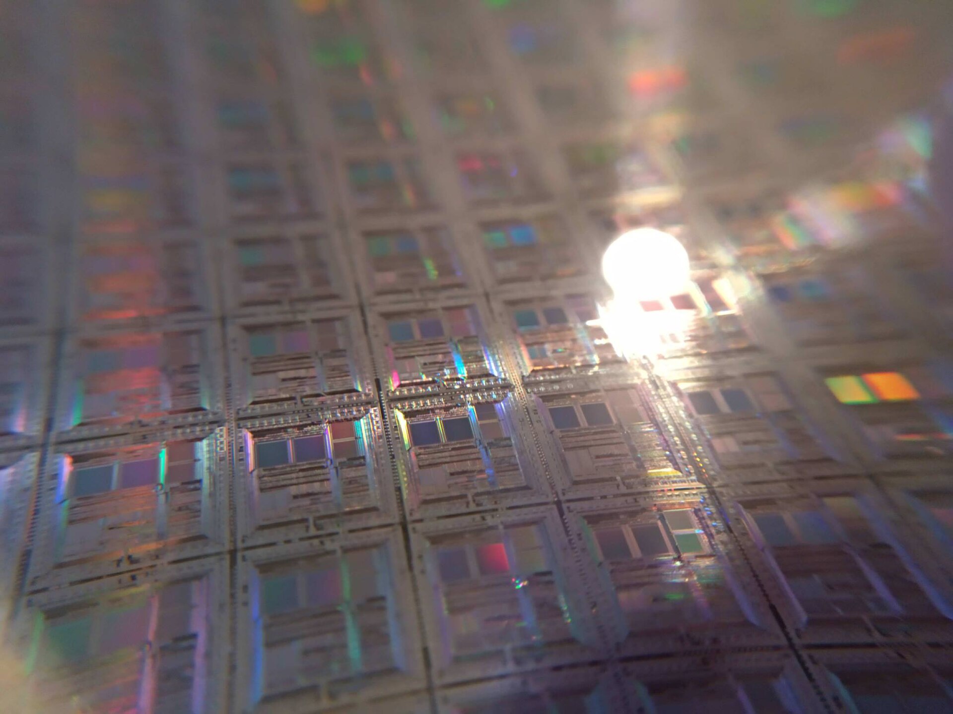
Advanced substrate and package engineering for high performance semiconductor platforms.
Explore domain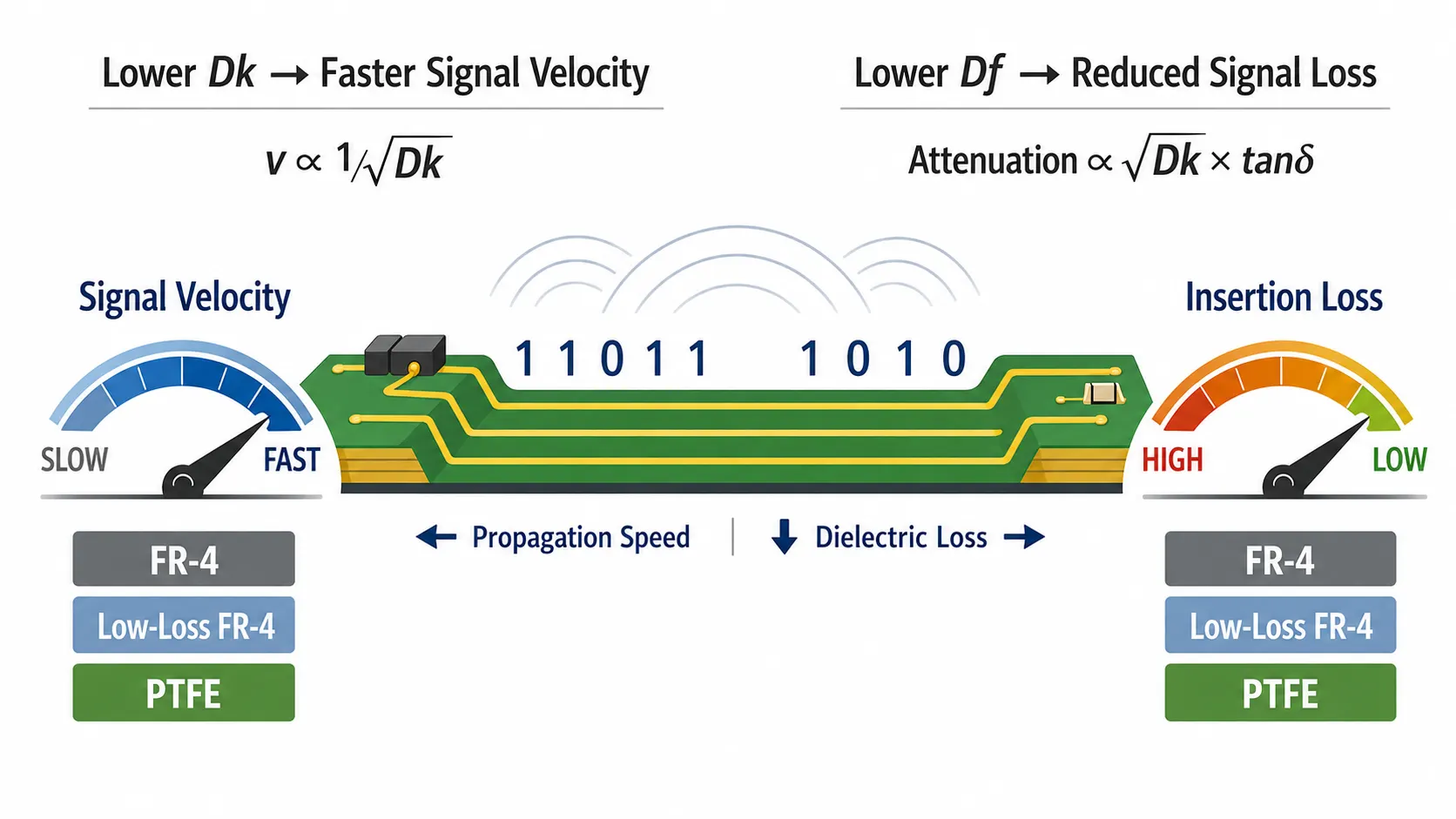
End-to-end SI and PI analysis for package, board, connector, and system-level performance optimization.
Explore domain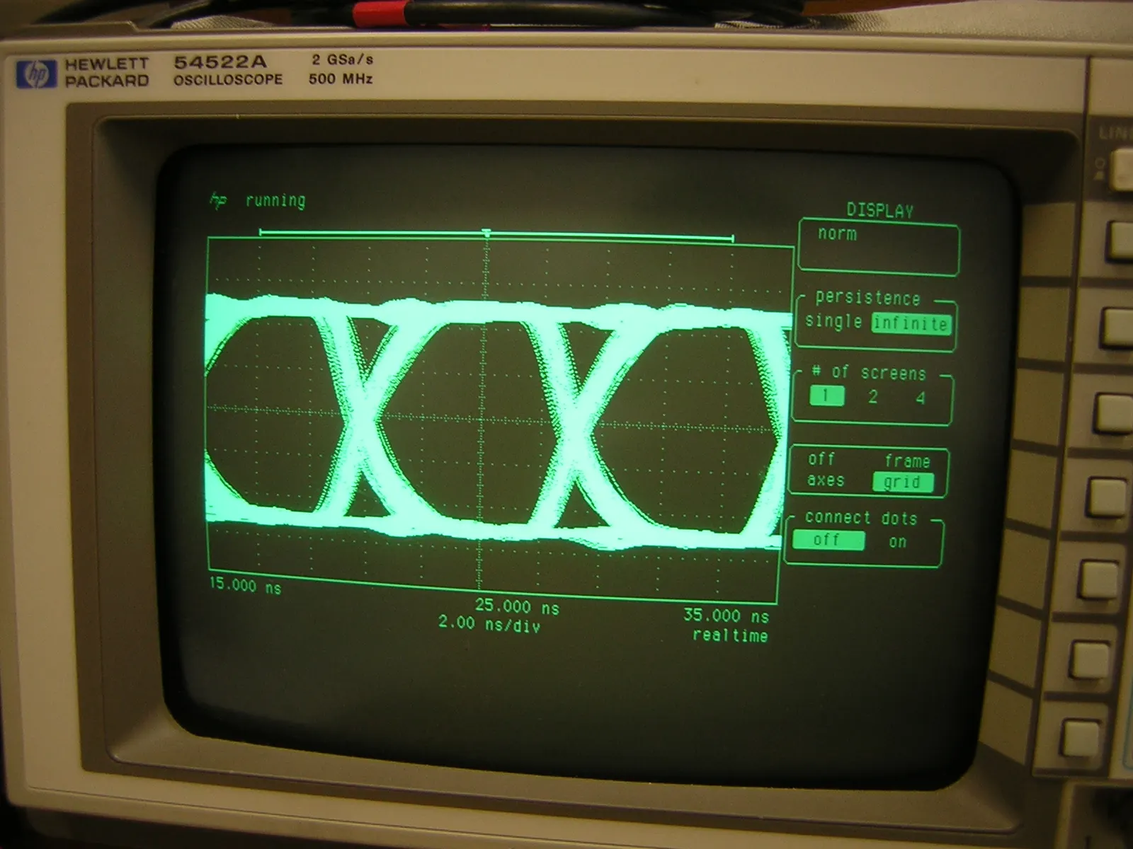
High speed serial channel engineering for next-generation semiconductor and compute platforms.
Explore domainEngineering support for silicon photonics integration, optical interfaces, and high-speed photonic test environments.
Explore domain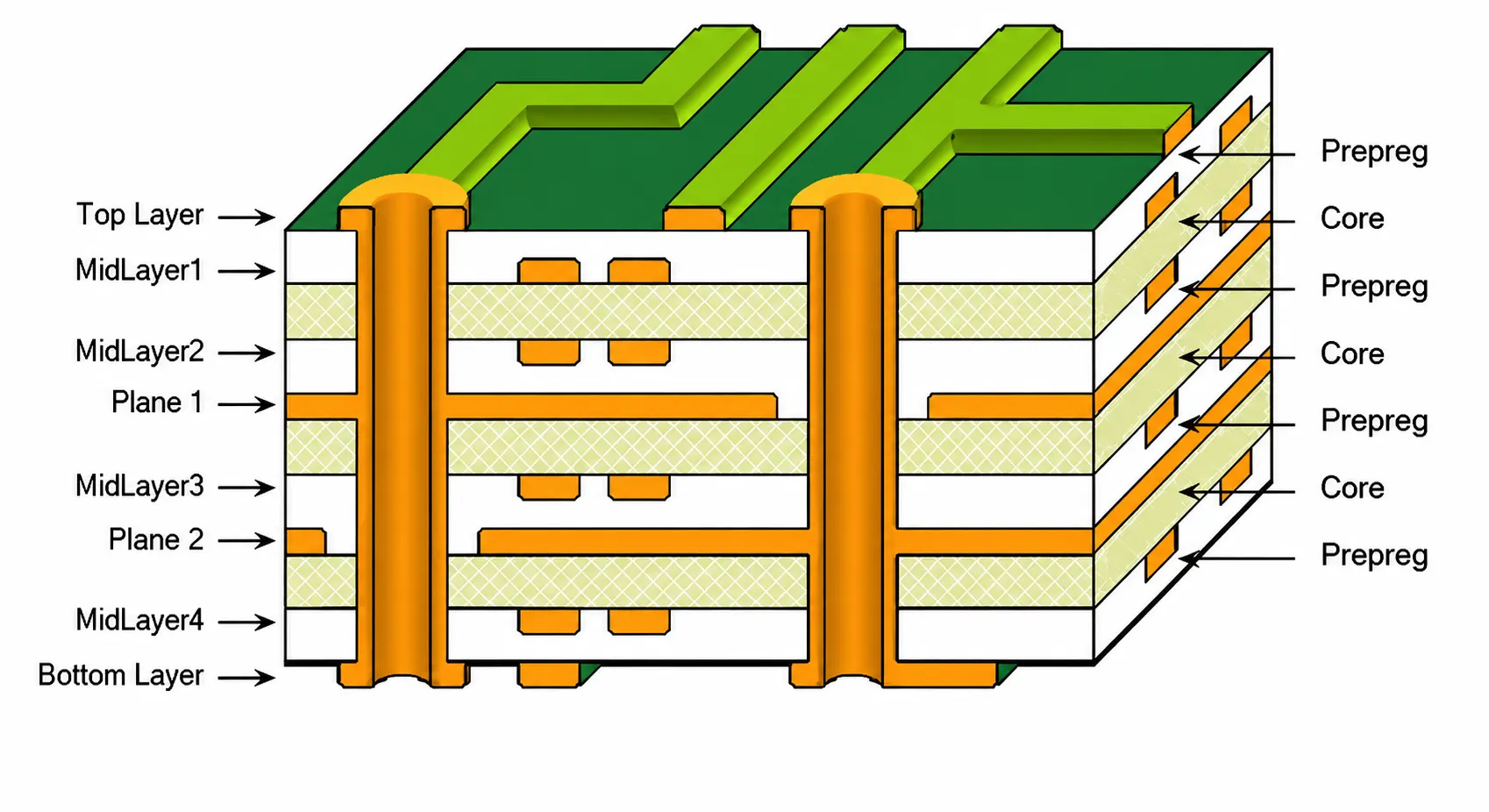
Transforming advanced engineering concepts into manufacturable and scalable semiconductor hardware platforms.
Explore domainDelivery Workflow
From requirements and design review through fabrication, assembly, qualification, and production support, SAS runs one structured delivery flow.
Program requirements, target specifications, compliance needs, and manufacturing assumptions are defined at the outset.
Package, board, RF, thermal, and mechanical engineering advance in one coordinated semiconductor development flow.
Fabrication, precision machining, PCBA, socket build, and subsystem assembly are executed against qualified production standards.
Electrical test, reliability, characterization, and qualification data are captured to verify performance before release.
Production transfer, sustaining engineering, documentation control, and change management support long-term delivery.
Product Focus
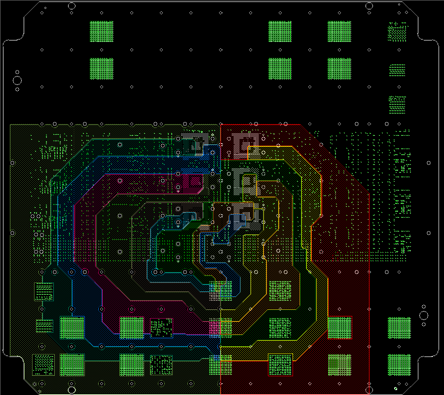
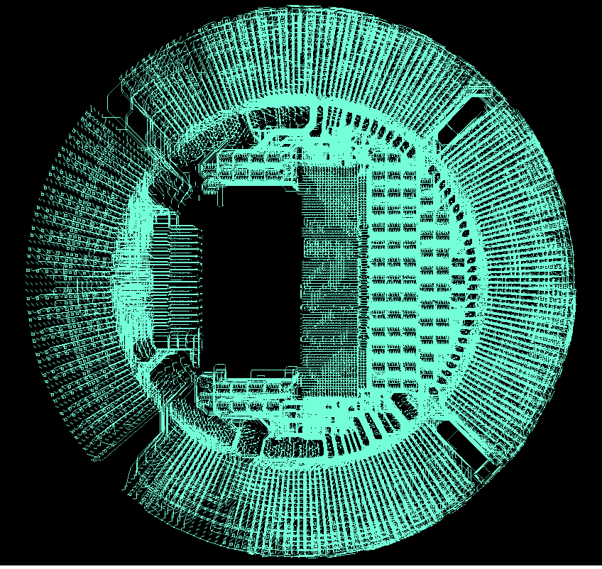
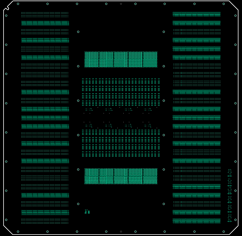
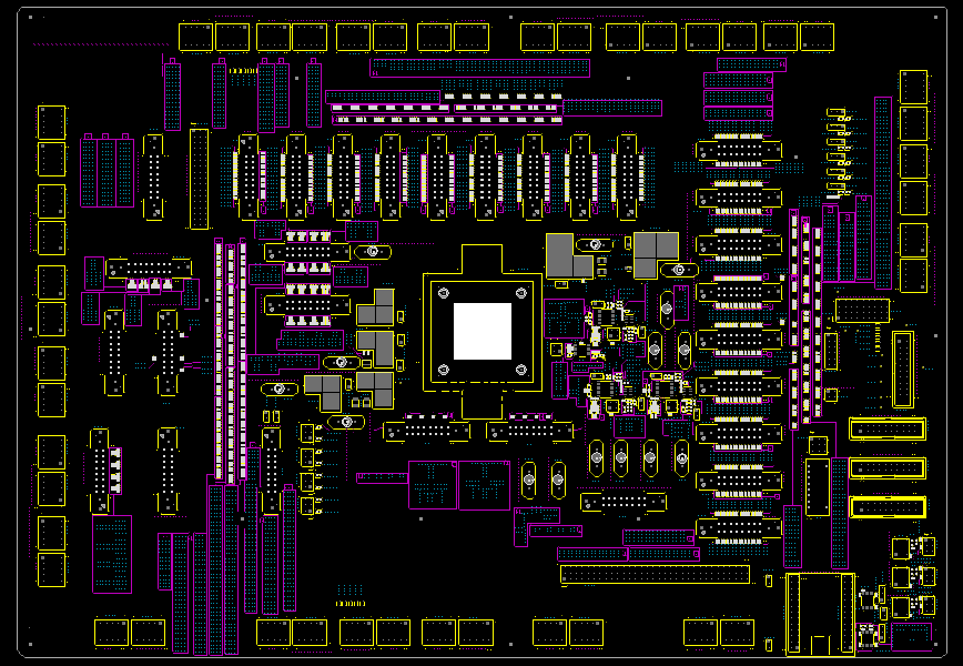
Representative semiconductor hardware programs delivered across SAS engineering, manufacturing, assembly, and test.
Global Engineering and Manufacturing Network
SAS operates across a global ecosystem of engineering, manufacturing, and supply chain partners, enabling efficient execution across regions and production environments.
South Korea
Korea Manufacturing Site
Incheon · GMT+9

High-reliability socket manufacturing, burn-in tooling, and semiconductor test hardware production for demanding device programs.
India
India Engineering Site
Bengaluru · GMT+5.5

Design engineering, PCB development, and DFX execution that help semiconductor programs move faster into production.
Taiwan
Upcoming Lane
Taipei · GMT+8
Taiwan partner onboarding is being prepared to extend SAS support for precision tooling, semiconductor fixtures, and production ramp execution.
Proof Layer
Customer programs across compute, networking, defense, medical, and sensing markets.















Next Step
Work with SAS to design, validate, and deliver advanced semiconductor hardware from concept to production.
Direct Contact
Ha-Marpe 3 st. Har Hotzvim, Jerusalem 9777403 Israel