


MLO and MLC substrate design
Engineering Domains/IC Package and Substrate Design
Engineering Domain
IC Package and Substrate Design
Advanced substrate and package engineering for high performance semiconductor platforms.
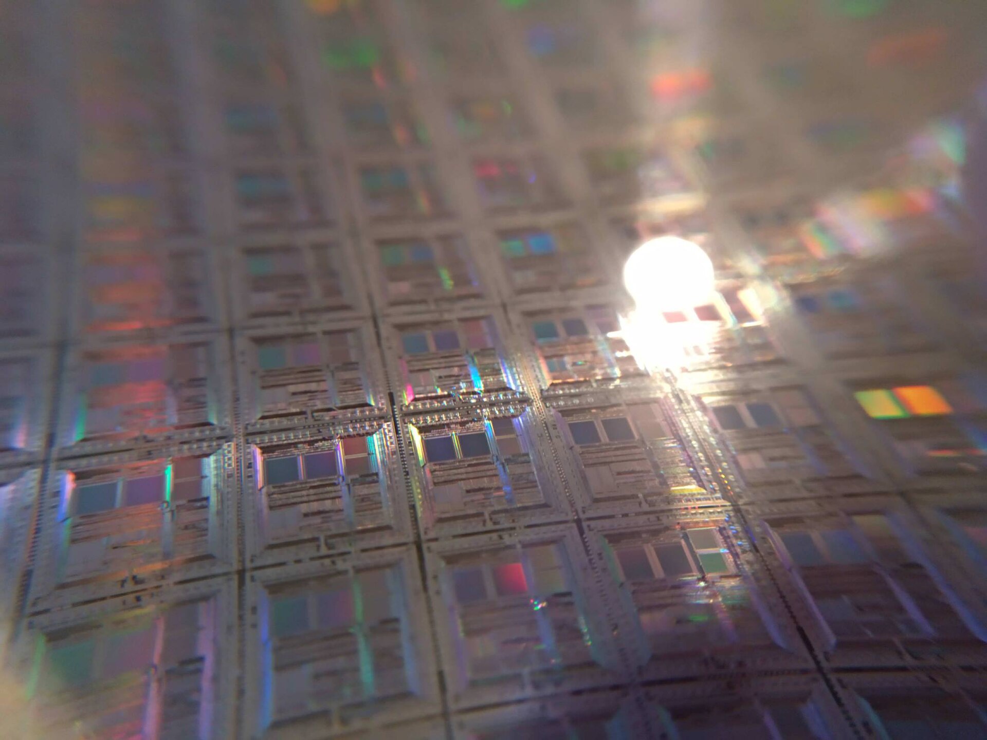
SAS supports advanced IC package and substrate development including MLO, MLC, hybrid substrate technologies, flip chip integration, wire bond implementation, and system-level package-board co-design.
Engineering Capabilities
What SAS Executes in This Domain
05
Capabilities
SAS
Execution CoreIC Package and Substrate Design
Flip chip support
Wire bond implementation
Package-board co-design
Multi-die integration
Engineering Model
Decisions That Keep the Program Buildable
Pinout shaped by system behavior
Bump, ball, and connector assignments are evaluated against channel topology, escape feasibility, power delivery, and board constraints.
Package and PCB co-design
Substrate layers, package breakouts, and board routing are reviewed together to prevent late interface conflicts.
Manufacturable substrate release
Design decisions are checked against supplier rules, routing density, via structures, solder mask, and assembly requirements.
Program Flow
From Definition to Release
Each domain page uses a practical flow that keeps design choices connected to implementation, review, and handoff.
01
Architecture definition
Clarify die configuration, interconnect map, package body, substrate type, signal classes, and board interface needs.
02
Assignment and escape
Plan bump, ball, and via assignments so power, high speed, control, and test groups can route cleanly.
03
Substrate implementation
Execute substrate routing, plane strategy, impedance structures, and manufacturability checks against supplier rules.
04
Release and supplier loop
Package the design for fabrication, respond to supplier feedback, and maintain a controlled revision path.
Release Package
Outputs Built for Review, Build, and Transfer
SAS structures domain work so the final handoff is practical for engineering review, supplier execution, lab bring-up, and controlled production transfer.
Package architecture and substrate layout data
Bump, ball, and pin assignment documentation
Substrate stackup and routing review package
Supplier-ready fabrication and assembly outputs
More Domains
Continue Across the SAS Engineering Stack
Engineering Domain
High Speed PCB Design
Constraint-driven multilayer PCB engineering for high speed compute, RF, mixed-signal, and advanced semiconductor platforms.
Engineering Domain
SI and PI Simulation
End-to-end SI and PI analysis for package, board, connector, and system-level performance optimization.
Engineering Domain
112G PAM4 and Advanced Interconnect
High speed serial channel engineering for next-generation semiconductor and compute platforms.
Engineering Domain
Silicon Photonics and CPO
Engineering support for silicon photonics integration, optical interfaces, and high-speed photonic test environments.
Engineering Domain
DFM and Production
Transforming advanced engineering concepts into manufacturable and scalable semiconductor hardware platforms.